MEMC LLC
A GlobalWafers Company
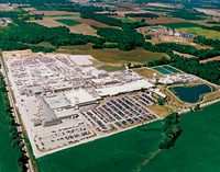
501 Pearl Drive
St. Peters, MO 63376
Tel: +1 636 474 5000
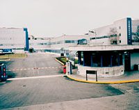
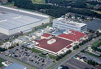
This facility has provided advanced-specification, large-diameter, polished, and epitaxial silicon wafer products for many of the world’s top device manufacturers.
Location
St. Peters, Missouri, USA (approximately 31 miles west of downtown St. Louis, Missouri)
Products
200mm and 300mm SOI substrates
SQUARE FOOTAGE
744,000
Quality/Safety Certifications
Quality Certifications; Safety Certifications
Background
The St. Peters Plant was built in 1959 by GlobalWafers (formerly, Monsanto Electronic Materials Company). This facility was the first merchant manufacturer of silicon wafers in the world - the first wafer produced was 19mm in diameter! Originally just a few acres in size, the facility now occupies 185 acres. The St. Peters Plant won the coveted "Missouri Quality Award" in 1994. This award is based on the same criteria as the Malcolm Baldrige National Quality Award, but at a state level. In 1995, the St. Peters Plant was recognized as one of the "Top Ten" manufacturing facilities in the USA by Industry Week Magazine.
Directions
From Lambert-St. Louis International Airport: Take I-70 West 15.3 miles to exit 220 (exit sign reads "Hwy 79/Elsberry/Louisiana"). At the top of the exit ramp, turn right onto highway 79 and go .08 miles to Pearl Drive exit (veer right, off highway 79). At the stoplight, turn left onto Pearl Drive and go .02 miles to MEMC Drive. Turn left onto MEMC Drive, veer left at the first fork in the road (the lake is now on your right). At the second fork, veer right. Visitor parking is at the top of the hill.
Transparency in Coverage
Link
This link leads to the machine-readable files that are made available in response to the federal Transparency in Coverage Rule and includes negotiated service rates and out-of-network allowed amounts between health plans and healthcare providers. The machine readable files are formatted to allow researchers, regulators, and application developers to more easily access and analyze data.